Email: sales@xtalong.com Tel: +86-28-80192520

Email: sales@xtalong.com Tel: +86-28-80192520
The Colpitts crystal oscillator circuit design uses two center-tapped capacitors in series with a shunt inductor to form its resonant tank to produce sinusoidal oscillations.
In many ways, the Colpitts Crystal Oscillator Circuit is exactly the same as the Hartley Oscillator we saw in other places. Just like a Hartley oscillator, a tuned oscillator circuit consists of an LC resonator circuit connected between the collector and the base of a single-stage transistor amplifier, producing a sinusoidal output waveform.

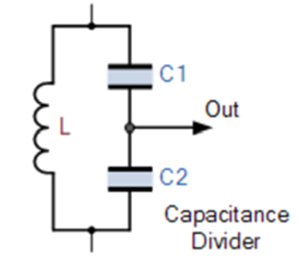
The Colpitts Crystal Oscillator Circuit is similar to the Hartley Oscillator, but this time the difference is that the center tapping of the oil tank circuit is now done at the junction of the "capacitive divider". network instead of the tapped autotransformer type inductor in the Hartley oscillator.
The Colpitts Crystal Oscillator Circuit uses a capacitive voltage divider network as its feedback source. Two capacitors C1 and C2 are placed on a single common inductor, L , as shown. Then C1 , C2 and L form a tuned tank circuit with the oscillation condition: X C1 + X C2 = XL , the same as the Hartley oscillator circuit.
The advantageous configuration of this type of capacitive circuit is that it has less self and mutual inductance in the resonant circuit, the frequency stability of the oscillator is improved, and the design is simpler.
Like the Hartley oscillator, the Colpitts Crystal Oscillator Circuit uses a single-stage bipolar transistor amplifier as the gain element, producing a sinusoidal output.
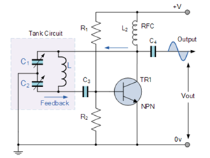
Consider the circuit below.

The transmitter terminal transistor is effectively connected to the junction of two capacitors, C1 and C2, which are connected in series and act as a simple voltage divider. When power is first applied, capacitors C1 and C2 are charged and then discharged through coil L. The oscillation across the capacitor is applied to the base-emitter junction and appears amplified at the collector output.
Resistors, R1 and R2 provide the DC bias that normally stabilizes the transistor in the normal way, while the additional capacitors act as DC blocking bypass capacitors. A radio frequency choke (RFC) is used in the collector circuit to provide high reactance (ideally open circuit) at the oscillation frequency (ƒr) and low resistance at DC to help start the oscillation.
The desired external phase shift is obtained in a similar manner as in the Hartley oscillator circuit, obtaining the positive feedback required for sustained undamped oscillation.
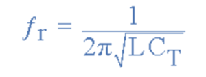
The amount of feedback is determined by the ratio of C1 and C2. These two capacitors are usually "joined" together to provide a constant amount of feedback, so when one is adjusted, the other automatically follows. The oscillation frequency of the Colpitts Crystal Oscillator Circuit is determined by the resonant frequency.
LC tank circuit, as follows:

where CT is the capacitance of C1 and C2 connected in series, given as:

The configuration of the transistor amplifier is a common emitter amplifier, and the output signal is 180o out of phase with respect to the input signal.
Since the two capacitors are connected together in series but in parallel with the inductor coil, resulting in an overall phase shift of zero or 360° for the circuit, the additional 180o phase shift requirement for oscillation is achieved. sup>o.
The amount of feedback depends on the values of C1 and C2. We can see that the voltage on C1 is the same as the oscillator output voltage Vout, and the voltage on C2 is the oscillator feedback voltage. Then the voltage on C1 will be much greater than the voltage on C2.
Therefore, by changing the capacitor values, C1 and C2 we can adjust the amount of feedback voltage returned to the tank circuit. However, a large amount of feedback may cause distortion of the output sine wave, while a small amount of feedback may not allow the circuit to oscillate.
The amount of feedback generated by the Colpitts Crystal Oscillator Circuit is then based on the capacitance ratio C1 and C2 which is the factor that controls the excitation of the oscillator.
This ratio is called the "Feedback Score", or simply:

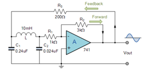
Colpitts Crystal Oscillator Circuit using op amps. Just like the previous Hartley oscillators, and using a bipolar junction transistor (BJT) as the oscillator active stage, we can also use an operational amplifier (op-amp). The operation of the op-amp Colpitts Crystal Oscillator Circuit is exactly the same as that of the transistor version, and its operating frequency is calculated in the same way.
Consider the circuit below.

Note the inverting amplifier configuration, the ratio of R2/R1 sets the amplifier gain. A minimum gain of 2.9 is required to start oscillation. Resistor R3 provides the required feedback for the LC tank circuit.
The advantage of the Colpitts Crystal Oscillator Circuit over the Hartley oscillator is that the Colpitts Crystal Oscillator Circuit produces a cleaner sinusoidal waveform due to the low impedance path of the high frequency capacitors. Also due to these capacitive reactance properties, FET-based Colpitts Crystal Oscillator Circuits can operate at very high frequencies. Of course, any op amp or FET used as an amplifier device must be able to operate at the required high frequencies.
The Colpitts Crystal Oscillator Circuit consists of an LC resonator oscillator circuit in parallel, the feedback of which is achieved through a capacitive voltage divider. As with most oscillator circuits, Colpitts Crystal Oscillator Circuits come in many forms, the most common being similar to the transistor circuit above.
The center tap of the can circuit is in a "capacitive divider" network that feeds a small portion of the output signal back to the transistor's emitter. The two capacitors in series create a 180° phase shift, which is inverted by another 180° to create the desired positive feedback.The oscillation frequency is a more pure sine wave voltage, determined by the resonant frequency of the resonant circuit.
If you want to learn more about it, please refer to this video: https://www.youtube.com/watch?v=CxRqx4jKtHU
Contact: Katya Vane
Phone: +86-18884136031
Tel: +86-28-80192520
Email: sales@xtalong.com
Add: No.4 of XinHang Road, West of High-tech zone, Chengdu City 611731, China
We chat