Email: sales@xtalong.com Tel: +86-28-80192520
Email: sales@xtalong.com Tel: +86-28-80192520
Nominal Frequency: 44.55MHz
Nominal Frequency Tolerance: ±2ppm
Frequency stability over temperature: ±2ppm
Temperature range: -40~85℃
SMD 3225 High-Frequency Stability TCXO
The SMD 3225 High-Frequency Stability TCXO (Temperature Compensated Crystal Oscillator) is engineered for
applications requiring exceptional frequency stability over varying temperature ranges.
This TCXO is ideal for telecommunications, GPS, and high-precision timing applications,
where maintaining accurate frequency is crucial.
Key Features:
High-Frequency Stability: The SMD 3225 TCXO offers outstanding frequency stability, ensuring reliable performance even in demanding environments.
Temperature Compensation: With advanced temperature compensation technology, this TCXO maintains its frequency accuracy across a wide temperature range, making it suitable for outdoor and industrial applications.
Compact Design: Its small 3225 footprint allows for easy integration into compact devices, optimizing space without compromising on performance.
Low Power Consumption: Designed for energy efficiency, the SMD 3225 TCXO minimizes power usage, making it perfect for battery-operated devices.
Applications:
Telecommunications
Global Positioning Systems (GPS)
Wireless Communication Devices
Automotive Electronics
Industrial Control Systems
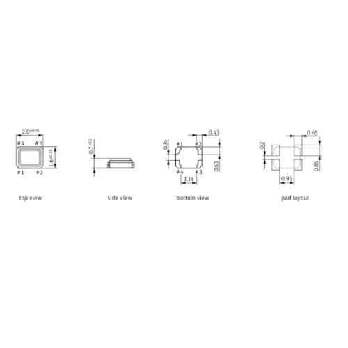
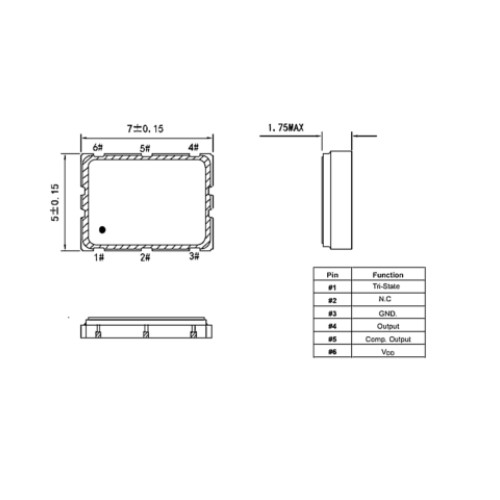
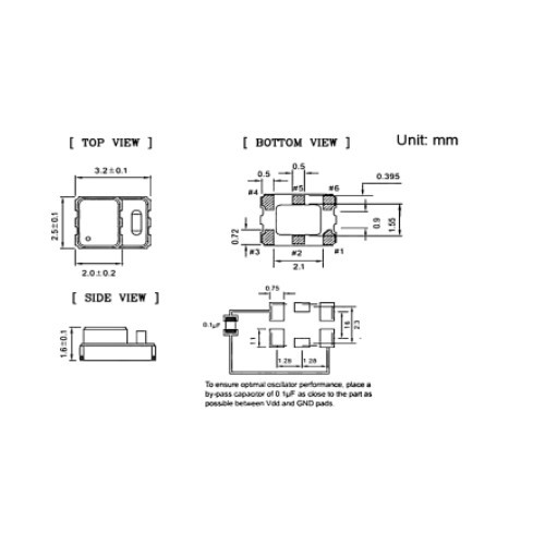
TCXO 3.2*2.5mm DIMENSIONS

PIN FUNCTIONS
| PIN | Function |
| #1 | NC |
| #2 | Tri-state |
| #3 | GND |
| #4 | Output |
| #5 | NC |
| #6 | Vdd |
FREQUENCY CHARACTERISTICS
| Parameter | Min. | Typ. | Max. | Units | Test Condition |
| Nominal Frequency | 44.55 | MHz | |||
| Nominal Frequency Tolerance | -2 | 2 | ppm | Frequency at 25°℃, 1 hour after 2 times reflow. | |
| Frequency stability over temperature | -2 | 2 | ppm | Referenced to the midpoint between minimum and maximum frequency value. | |
| Temperature range | -40 | 85 | ℃ | The operating temperature range over which the frequency stability is measured | |
| Supply voltage stability | -0.2 | 0.2 | ppm | Supply voltage varied ±5% at 25 °℃ | |
| Aging | -1 | 1 | ppm | first year at 25°℃ | |
POWER SUPPLY
Parameter | Min. | Typ. | Max. | Units |
Supply voltage | 3.135 | 3.3 | 3.465 | V |
Current | 40 | mA |
OSCILLATOR OUTPUT
Parameter | Mini | Type | Max | Unit | Test Condition |
Output waveform | CMOS | ||||
Output voltage level high | 2.97 | V | |||
| Output voltage level low | 0.33 | V | |||
| Output load capacitance | 15 | pF | Operating range | ||
Duty cycle | 45 | 50 | 55 | % | Measured at 50% VDD trigger level |
Rise and fall times | 3 | ns | CMOS logic output at 10% to 90% | ||
Start time | 5 | ms | |||
| Tri-State Output Active | 2.31 | V | |||
Tri-State Output in High-Impedanc | 0.99 | V |
JITTER
| Parameter | Mini | Type | Max | Unit | Test Condition |
| RMS Phase Jitter | 1.5 | pSec | (12KHz-20MHz) |
TCXO oscillator test circuit

OUTPUT WAVEFORM

RECOMMENDED IR REFLOW PROFILE
IR REFLOW PROFILE OF CERAMIC SMD PRODUCTS FOR Pb FREE PROCESS

联系人:Katya Vane
手机:+86-18884136031
电话:+86-28-80192520
邮箱:sales@xtalong.com
地址: No.4 of XinHang Road, West of High-tech zone, Chengdu City 611731, China