Email: sales@xtalong.com Tel: +86-28-80192520

Email: sales@xtalong.com Tel: +86-28-80192520
Jitter reflects the time deviation of a digital signal from its desired location. The bit cycle of high-frequency digital signals is very short, generally in hundreds of ps or even dozens of ps. A small jitter will cause the change of signal sampling position level, so high-frequency digital signals have strict requirements for jitter.
The actual signal may have high complexity, such as both a random jitter component (RJ) and a deterministic jitter component (DJ) with different frequencies. Deterministic jitter may be caused by intercode interference or some periodic interference, while random jitter is largely caused by noise on the signal. Generally, we judge the state of the digital signal that exceeds the threshold as "1", and the state that is below the threshold as "0". Since the rising edge of the signal is not infinitely steep, the vertical amplitude noise will cause the left and right changes when the signal crosses the threshold point, which is the reason for signal jitter caused by noise.
To analyze the signal jitter, the most commonly used tool is the broadband oscilloscope with the response of the jitter analysis software. The dither analysis software in oscilloscope can easily decompose the size and various components of the dither. But many high-speed chips now require clock jitter of less than 1ps or less. This requires the help of other measurement methods, such as phase noise measurement methods.

Phase noise:
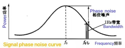
In the frequency domain, the data offset is defined by phase noise. For the clock signal frequency for the f0, if without dithering signals, the signals of all power points should be focused on the frequency f0, because any signal jitter, some of these jitter is random, some is certain, distributed in quite a wide frequency band, so the emergence of the jitter will enable signal power is extended to the band.
The phase noise of the signal is the power components of the signal at a particular frequency, and the curve connecting these components is the phase noise curve. Phase noise is usually defined as the dBc/Hz value at a given offset, where dBc is the ratio of the power to the total power at that power in dB. For example, the phase noise of an oscillator at a certain offset frequency is defined as the ratio of the signal power in the 1Hz bandwidth to the total signal power at that frequency, that is, the ratio of the area in the 1Hz range at the FM frequency to all the areas at the whole noise frequency.
It can be seen from the phase noise graph that most of the jitter is concentrated near the frequency f0. The farther the frequency band from F0, the smaller the jitter energy. The following example illustrates the clock input requirements:
The RMS JPER (12 KHZ ~ 20 MHZ) : 0.5 ps
Phase noise (10-100 KHZ) : -120 DBC /Hz
This is actually two requirements, one is required in the frequency band 12kHz~20MHz, RMS jitter should not be greater than 0.5ps. The other aspect requires that the power spectral density at any frequency point in the frequency range of 10~100kHz should not exceed -120 DBC /Hz.